
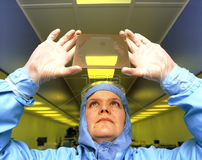
Visual inspection of a photomask used in the fabrication of integrated circuit wafers at Seagate Microelectronics Ltd, Livingston, Scotland. The photomask is used in a photolithography process to selectively etch an electronic pattern onto a wafer of crystalline silicon - the base material for the ultimate integrated circuits that will be die stamped from the completed wafer.
| px | px | dpi | = | cm | x | cm | = | MB |
Details
Creative#:
TOP10230126
Source:
達志影像
Authorization Type:
RM
Release Information:
須由TPG 完整授權
Model Release:
N/A
Property Release:
N/A
Right to Privacy:
No
Same folder images:
 Loading