
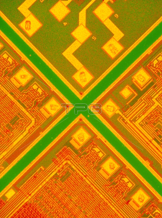
Light micrograph showing the junction of 3 memory silicon chips & a test module (top) on a manufac- tured wafer. Chips are made on thin, circular, silicon wafers 7.5cm in diameter. Each wafer forms a substrate on which about 100 chips are made by a series of coating & etching processes that build up the chip's complex circuitry. Electronic probes are lowered onto the test module's square pads for quality control testing. The chips are cut from the wafer by running a diamond knife along the green bands between each chip. The 16K 4116 chips in this micrograph are typical memory chips used in computers & other electronic equipment. Mganif- ication: x20 at 35mm size, x40 at 6x7cm size. Ref: MICROCOSMOS, fig. 8.20, p. 160
| px | px | dpi | = | cm | x | cm | = | MB |
Details
Creative#:
TOP10230009
Source:
達志影像
Authorization Type:
RM
Release Information:
須由TPG 完整授權
Model Release:
N/A
Property Release:
N/A
Right to Privacy:
No
Same folder images:
 Loading